
Earlier articles were about "how to simplify a circuit" — Thévenin, Norton, Kirchhoff, Superposition, and one that explained the MOSFET as a water gate. This one goes one level deeper: how to create a current that is "exactly what you said it would be" in a circuit, and copy it out in proportion.
This operation is called a current mirror. The name sounds fancy, but it is actually the cheapest and most common building block in analog circuits; three generations of it can be drawn on a single page — I've put my own one-page sketch at the end of the article.
Story: The Copying Trick on Mirror Lake
The castle needed to build a water-distribution tower: a water meter () on the main channel, and three other channels supplying the water mill, the dye works, and the vegetable garden, each of which had to deliver no more and no less than exactly two, four, and eight times the main channel's flow.
Fox Ali's clumsy idea was to install a water meter on every channel and assign someone to watch and adjust the gate. Grandpa Copper-Nail shook his head: how many meters and how many people would that take?
He took Ali to the edge of Mirror Lake. The surface was as flat as a sheet of glass; the willows on the bank, the tip of the tower, and Ali himself were all reflected clearly in the water.
When you raise your left hand, the reflection raises its left hand; when you step forward, the reflection steps forward. Nobody taught it to do that. Because the water surface is flat, the reflection is guaranteed to be exactly the same.
Ali understood: as long as the two channels have the same gate opening and the same water path behind the gate, then however much water one channel takes in, the other channel will deliver the same amount. The gates are connected by a shared gate rod — no water flows through that rod; it only transmits the "opening".
In circuit terms:
- Gate opening = gate-source voltage ;
- Gate rod = a shared gate trace (which hardly consumes any current);
- Water flow = drain current ;
- Water-path width = width-to-length ratio .
So the entire content of the current mirror is one sentence: share one , and the current is copied over in proportion to .
But the lake surface is not always flat. When the wind blows (when the output voltage changes), the reflection distorts. The difference among the three generations of gatekeepers all comes down to "how to make the reflection resist the wind".
1. First, Write the "Copying" as a Formula
A MOSFET in saturation:
Let the overdrive be and ; the expression above becomes .
The transistor on the left (M1) must be connected to itself: its gate is tied to its own drain. In this way it "finds" a by itself, such that the flowing into it can pass through exactly:
This step is the foundation of the entire current mirror: the reference current needs no "standard" at all; it sets the gate voltage by itself. This also explains why M1 must be diode-connected — without being given a , it doesn't know how far to open.
The transistor on the right (M2) has the same gate voltage and its source is likewise grounded, so ; dividing the two equations:
If (the transistor is "ideal"), only that clean ratio remains:
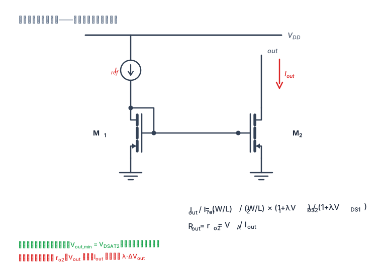
Figure 1: M1 connects to itself and translates into ; M2 copies this and outputs . The ratio depends only on , and all the error lives in those two terms.
First calculation: some concrete numbers
Take a set of "textbook process" parameters; all the worked examples below use them:
| Parameter | Value | Notes |
|---|---|---|
| Mobility × oxide capacitance | ||
| Threshold voltage | ||
| Channel-length modulation coefficient, | ||
| Reference current | ||
| Unit device | ||
| Two unit devices in parallel |
First calculate M1's overdrive and gate voltage:
Ideally . That is the "two-times mirror".
Along the way we get two quantities that will be used repeatedly later:
is the "leak gap" of this branch: an ideal current source has ; the real one only has .
Second calculation: exactly how accurate is this "two times"
M1's drain voltage is its own , while the output is held at by something else, so:
This is not "built wrong"; it is "copied wrong" — because the two transistors have different , channel-length modulation makes their water paths slightly different in width. This is the ceiling of the simple current mirror.
2. Why the Reflection Distorts: Channel-Length Modulation Is a "Leak Gap"
The physical picture is straightforward: the higher the drain voltage, the more the channel pinch-off point moves toward the source, the effective channel length shortens, the equivalent resistance decreases, and the current increases. In terms of , it is exactly that .
For a current mirror, the most critical quantity is the output resistance, that is, "if the output voltage changes by 1 V, how much does the current change":
Plugging in numbers: the output swings from 0.7 V to 1.7 V ():
A 1 V swing costs 5% current error. For a current source biasing a DAC or a sensor, this is already unacceptable.
Can we save it by "making the transistor longer"? Yes — roughly decreases as , and grows accordingly. But a large brings bigger area, parasitic capacitance, and higher minimum operating voltage — and a single transistor's will always remain on the order of one ; to gain another order of magnitude, you have to change the structure.
3. Hang a Curtain in front of the Mirror: Cascode
Grandpa Copper-Nail's approach is simple: hang a curtain in front of the mirror so the wind only hits the curtain.
Specifically: stack another transistor M3 on top of M1 (also connected to itself), stack M4 on top of M2, and connect M4's gate to M3's gate. M3 and M4 are that curtain, known as cascode.
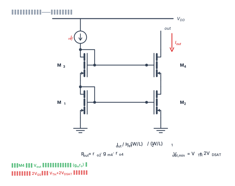
Figure 2: M4's source is M2's drain. M4 is in "common-gate" configuration; its source voltage is locked by the gate voltage and barely moves with — M2's is thus pinned.
Why the curtain works
M4 operates in the active region; its source voltage is about . As long as is still high enough, M4 holds this voltage steady. Almost all of the change falls across M4's drain-source, not on M2. Since M2's doesn't move, naturally doesn't move either.
Seen from a small-signal perspective it is also clean: the resistance looking upward from M2's drain is multiplied by about by the common-gate stage:
Plugging in numbers (, ):
From 100 kΩ to 20 MΩ, a full 200 times. For the same 1 V swing, the current error drops from to:
By the way, note a general conclusion: is the transistor's intrinsic gain (here ), and the cascode raises the output resistance by "one intrinsic gain". This is the same reason a cascode can boost amplifier gain.
The curtain's price: headroom
The curtain is not free. M3 is connected to itself, so its gate is pushed to ; for M4 to stay in saturation, its drain (which is the output) must satisfy
That is, the output voltage must be at least 0.9 V, otherwise M4 falls into the linear region, the curtain fails, collapses in an instant from 20 MΩ to a few kΩ, and the current runs away.
In a 1.8 V supply, 0.9 V means only 0.9 V is left for the signal; in a 1.2 V supply, only 0.3 V remains — basically unusable. This is why in many low-voltage circuits, cascode is actually "worse" than the simple mirror.
4. Hang the Curtain One Notch Lower: Wide-Swing Cascode
The contradiction is clear: the curtain stabilizes the current, but the curtain itself demands a share (it eats headroom).
Where is it eaten? In M3's gate being pushed to : , while M4's source only needs . A large part of that on the gate is given away for nothing.
Grandpa Copper-Nail moved the curtain's hanging point one notch lower: don't let M3 connect to itself; instead, give it a bias voltage that is "just enough".
In this way M4's gate is only 0.9 V, and its source (M2's drain) only needs 0.2 V, so:
The same curtain, the same 20 MΩ output resistance, but the minimum output voltage drops from 0.9 V to 0.4 V — gaining a full of headroom for free. This is the "wide-swing cascode".
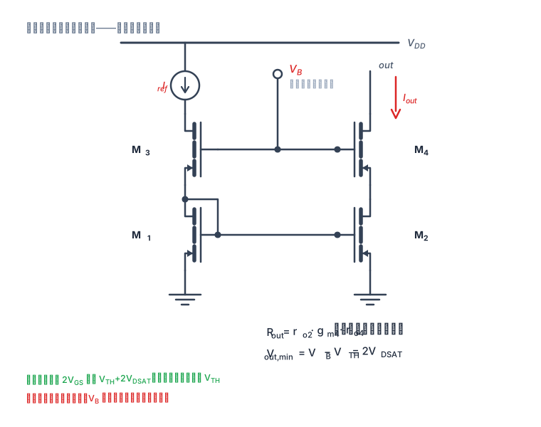
Figure 3: M3's gate is no longer connected to its own drain; instead, an extra bias branch supplies . The cost is exactly that extra branch — and all the trouble it brings.
How Is Made
A clever resistor-free method: take a transistor whose W/L is only 1/4 of the cascode transistor's, and run the same current through it.
With W/L scaled down to 1/4, the overdrive exactly doubles: , so the gate voltage of this diode-connected transistor is
A small current branch plus a "deliberately narrow" transistor produces . (In practice, engineers also use a " with a resistor in series" or a source-follower version; in essence they all create the level.)
The Cost List (This Section Matters More Than the Formulas)
- One extra bias branch: a bit more current, a bit more noise, a bit more area, and one more trace that must be matched;
- must track process corner and temperature: if is too high, the headroom saved is wasted; if too low, M4 enters the linear region and collapses. So that 1/4-width transistor must be the same type, same orientation, and placed closely to the cascode transistors;
- The bottom transistor of the reference branch must be handled: in my sketch I drew M1 as connected to itself (schematic drawing). In a rigorous implementation, the bottom transistor of the reference branch should also have its held near ; otherwise it pushes its own up to and gives back half of the saved headroom — a common practice is to also route separately from a bias branch.
5. Comparison Table of the Three Generations
| Simple | Cascode | Wide-swing cascode | |
|---|---|---|---|
| Transistor count | 2 | 4 | 4 + bias branch |
| Mirror ratio | Same | Same | |
| Output resistance | |||
| Usable headroom at 1.8 V | 1.6 V | 0.9 V | 1.4 V |
| Current error for a 1 V swing | 10 µA (5%) | 0.05 µA (0.025%) | 0.05 µA (0.025%) |
| Extra requirements | None | None | Bias branch + matching |
| Good for | Large headroom, moderate accuracy | High-voltage margin, high resistance | Low voltage, both stable and wide |
| Typical uses | Digital circuit biasing, rough current limiting | High-voltage amplifier loads | Low-voltage amplifiers, DACs, sensors |
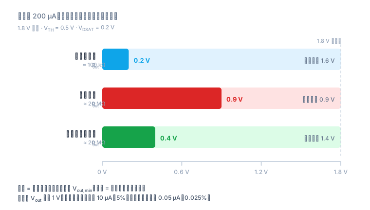
Figure 4: The dark color is the voltage that "must be given up"; the light color is the headroom available for the signal. The cascode's 20 MΩ costs 0.7 V of headroom — in a 1.8 V supply, that trade starts to become unfavorable.
6. Trial: 1.8 V, 200 µA, ±1% Error
Now let's put the above together and make a real choice. Requirements:
- Supply 1.8 V, output current (obtained by mirroring two times);
- The output voltage varies between 0.5 V and 1.5 V (determined by the following stage);
- Current error over the whole range ≤ 1% (i.e., ).
Step 1: Translate "error" into "output resistance"
Compare the three generations: the simple mirror gives 100 kΩ (short by 5×, disqualified); both cascode and wide-swing give 20 MΩ (40× margin, qualified).
Step 2: Translate "headroom" into "minimum output voltage"
Cascode needs 0.9 V (disqualified — at 0.5 V, M4 has already fallen into the linear region); wide-swing needs 0.4 V (qualified).
Conclusion: choose the wide-swing cascode. Note that this conclusion is not "wide-swing is more advanced" but "the 1.8 V supply cannot fit the 0.9 V step". If this circuit ran on 3.3 V and the output went no lower than 1.5 V, a plain cascode would do, and you'd save an entire bias branch.
Step 3: Calculate Device Sizes (with 0.2 V Overdrive)
That is, and ; , , ✓.
Step 4: What Really Stops You Is Not λ, but Mismatch
Many people stop here — but all the calculations above assume "the two transistors are identical". In reality they are not; the threshold voltage has random deviation, described by Pelgrom's law:
And this deviation becomes current error without attenuation:
Note the factor : the smaller the overdrive, the more deadly the mismatch. At it equals — that is, a 1 mV threshold deviation produces a 1% current deviation.
Let's verify with the first step's mirror (area ):
is 4.7% — far from ±1%. To get 3σ ≤ 1%, we need:
On top of that, the 1:2 mirror using three unit devices in parallel (two in M2, one in M1) brings a factor of amplification, so the area needs to be about
The transistor goes from 10 µm × 1 µm to 60 µm × 6 µm — a 36× increase in area. And this is the result of "giving the entire budget to mismatch"; if itself only achieves 1%, the error budget must be split and the area grows even more — area grows inversely with the square, and the more aggressive the accuracy target, the more exponential the price.
Three Teaching Points from This Section
- Choose the structure by headroom: is a hard threshold; if it doesn't fit, it doesn't fit;
- Size by accuracy: λ sets the ceiling of the structure, while mismatch decides whether you can ultimately meet the spec;
- Ratio mirrors should be built from "unit devices": 1:2 means two identical devices in parallel, not drawing one device twice as wide — the latter inevitably introduces systematic offset from orientation, stress, and gradient in layout.
7. The Two Main Sources of Error in Current Mirrors (Everything Else Is a Variant of These)
1. Systematic error: channel-length modulation (unequal )
The error caused by can be calculated, and it can be compensated:
- Increase (, the most direct, but takes area);
- Use cascode (pin ; the error becomes on the order of );
- Or use feedback to force the two transistors' to be equal (the most common trick in current sensing).
2. Random error: mismatch
Mismatch cannot be eliminated; it can only be "traded for area": . Engineering practices:
- Unit device arrays: build all transistors from the same unit cell; 1:N is simply N in parallel;
- Same orientation, same environment: keep the channel direction of all transistors identical to avoid stress/mobility anisotropy;
- Common-centroid layout: interleave (ABBA / 2-D interleaving) so that linear process gradients cancel each other;
- Add dummies: place a non-functional identical transistor at each end so the edge devices have the same neighbor environment;
- Place them close together: temperature gradient, well potential, and STI stress all decay with distance;
- Don't cross wells/regions: don't put one transistor in an isolation region and another on the substrate.
An Often-Overlooked Trap: The Current Mirror Is Only "Stiff" at Low Frequencies
20 MΩ looks strong, but there is also capacitance at the output. with :
Above 4 kHz, this "20 MΩ constant current source" starts to soften, and by a few hundred kHz it mostly behaves like a few kΩ. So the high-frequency "stiffness" of a current source never comes from the cascode, but from loop bandwidth / decoupling / local feedback. Don't use DC formulas to explain switching-transient behavior.
8. Five Real-World Scenarios
1. Op-amp / OTA biasing and active loads
Every differential pair needs a tail current source (which sets and common-mode rejection), and the active load is also a current source. With a cascode load, the gain goes from
to . This is the most classic appearance of the cascode in analog circuits.
2. Current-steering DAC
Each bit is a switch plus a unit current source; the output resistance of the current source directly determines the INL: changes with the output node voltage → different codes give different output impedances → nonlinearity. That's why the unit current sources of high-speed DACs are almost universally cascode (or regulated cascode), with matching ensured by "thermometer decoding + unit device arrays".
A rough estimate for a 10-bit requirement: the LSB relative accuracy is about . Working backward with the formula above,
Each unit current source is 2500 µm², and a 10-bit DAC has 1023 of them — this is why high-resolution DACs use segmentation (thermometer coding for the upper bits) and calibration rather than brute-force stacking of area.
3. Bandgap reference / PTAT biasing
The PTAT current in a bandgap needs to be copied by current mirrors to several branches (core, output, buffer). The biggest concern here is startup: a self-biased current mirror has a "zero-current" degenerate solution (all transistors off, the circuit "quietly dies"), so a startup circuit must be added to kick it out of that state.
4. Sensor constant-current biasing
PT100/PT1000 are excited with 1 mA constant current (to limit self-heating), and the same applies to photodiodes, strain bridges, and Hall sensors. The value of a constant-current source is that "lead resistance does not enter the result": with no voltage-drop variation across the series lead resistance, the reading is unaffected by lead length. Here the higher the output resistance the better, and a 1 kΩ lead resistance is completely negligible against 20 MΩ.
5. Current sensing / 1:N mirroring
In load switches and motor drivers, a 1:1000 mirror transistor "peeks at" the current of the power transistor. There is a classic mistake here: the power transistor's is only 50 mV (on-state drop), while the mirror transistor's is 300 mV — a difference of 250 mV. λ alone introduces
of systematic error, larger than the accuracy you want to measure. The industrial practice is to use an op-amp to force the two transistors' drain voltages equal (sense FET), or simply use a cascode to pin both ends to the same potential.
9. Seven Pitfalls Checklist
- Only memorizing the ratio formula while ignoring : unequal is a source of hundreds of mV of error.
- Thinking cascode raises the accuracy ceiling: it only raises ; mismatch is not improved at all ( is unchanged, and the deviation remains).
- Forgetting the cascode's "high-frequency failure": the output pole may be only a few kHz.
- Forcing cascode on a low supply: once is exceeded, collapses from MΩ to kΩ — worse than the simple mirror.
- Ignoring the body effect: in an NMOS cascode, the top transistor's source is not grounded, so is raised and must be recalculated; either use a deep n-well or switch to a PMOS version.
- Forgetting the startup circuit: the zero-current degenerate point of a self-biased current mirror makes the whole chip "quietly not work".
- Noise is copied along too: the mirror copies the reference branch's noise proportionally, and the cascode does not make it quieter. For a branch with and , the thermal-noise current density is about
which over a 1 MHz bandwidth is about — for measurements at nA-level accuracy (such as fA-level current measurement), this number is fatal.
10. One-Line Wrap-Up
A current mirror = a shared gate voltage. All the remaining effort goes into handling the fact that "the two transistors are actually not identical":
- Different → pin it with cascode (cost: headroom);
- Different → use wide-swing bias (cost: one branch);
- Different → trade for area and layout (cost: bigger and slower);
- Different frequencies → fill the gap with feedback and decoupling (cost: design complexity).
What's truly hard is never drawing those two transistors, but knowing at which step to concede: if the 0.9 V step doesn't fit in 1.8 V, then honestly draw one more bias branch.
Appendix: My Sketch
Below is the sketch I drew at the time, three diagrams from left to right: simple, cascode, and wide-swing cascode. The formulas and pros/cons are jotted down casually and can be compared with the derivations in the main text.

Sketch: simple (), cascode (), wide-swing ( supplied by an extra branch, ).
If you only want to remember one sentence: "Cascode buys output resistance and pays with headroom; wide-swing simply cuts one off that bill."